
Introduction
When a motherboard is rendered completely irreparable—whether due to liquid damage, short circuits, or physical impact—the device typically fails to power on; however, the core NAND flash memory chip often remains intact, thereby preserving the opportunity for data recovery. By employing specialized board-level data recovery techniques, technicians can bypass the damaged motherboard to directly access the contents of the storage chip, enabling the extraction of critical data such as photos. Utilizing NAND programmers and data read/write tools to perform low-level operations, repair professionals can execute chip-level data recovery—a vital solution for retrieving data in cases where the motherboard has sustained severe damage.
Understanding the Causes of Motherboard Damage and Image Loss
When a motherboard fails, the most not unusual symptom is a completely dead device that doesn’t work, turn on, or show any signs of life. However, in many cases, the NAND storage chip that holds your images is still physically high quality. The problem lies within the power system or logic circuits, now not the memory garage itself, which enables recovery through direct chip access.
Image loss usually occurs because the operating system cannot boot to access internal storage, not because documents have been deleted. Heat damage during prolonged charging, liquid corrosion, or voltage spikes can disconnect critical circuits. Understanding this helps technicians retrofit the device at the board level instead of replacing it entirely, which is the first step in expert data medicine workflows .
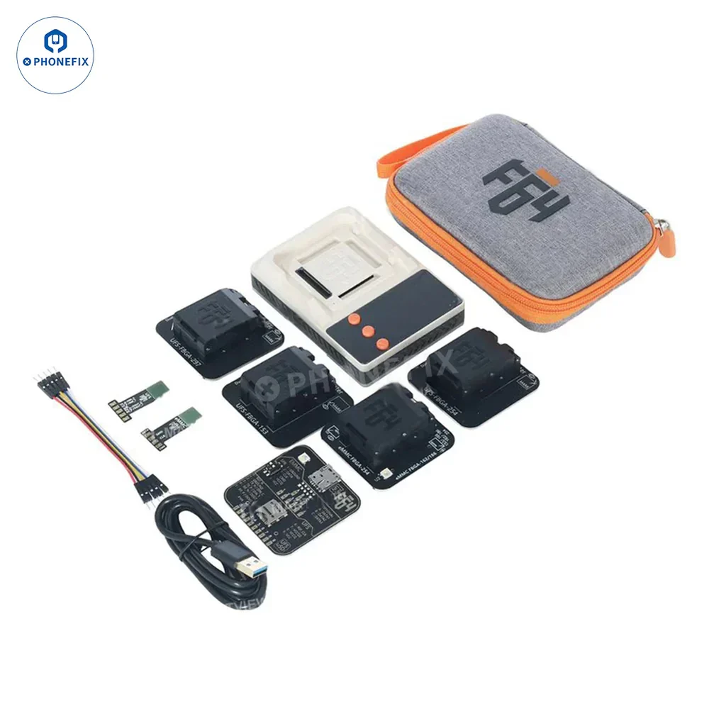
Equipment and preparations required for government-level data recovery
Before you begin, proper training is essential for a safe and successful recovery. A specialized setup includes a hot air recovery station, microscope, PCB holder, power (preferably no smooth or low residual current like Amtech 559), soldering iron, tweezers, and NAND programmer A very good data transfer cable is also required to connect the programmer to the rail.
The workplace shall be accessible, antistatic and properly illuminated. Technicians usually set newer air settings to 330°C to 380°C depending on board thickness and chip type, although as a shield of airflow to keep adjacent connectors away from lifting curved odd tweezers for single chip control, ensure no damage through the NAND remote.
Safe Distancing and Identification of the NAND Storage Chip
The first technical step is to carefully disassemble the damaged device and disassemble the motherboard. Once removed, the underside of the panel should be inspected under a microscope for rust, burn areas, or cracked additives. Cleaning the table with isopropyl alcohol improves visibility and ensures better control of heating.
The NAND chip is usually located near the CPU or under a protective metal cover. It is a BGA (Ball Grid Array) chip that stores all personal data which includes photos and device files. It is important to identify it effectively, as removing the wrong chip can cause a permanent loss of capacity. During this step, technicians also check for board distortion or weak solder joints before applying heat.
Using a hot air rework station to remove tile
Once the NAND chip is installed, current is applied around the edges to help distribute heat quietly and protect the PCB. The hot air conversion station is then set to approximately 360°C with controlled airflow. The heating process is completed in a circular motion to prevent overheating of an area that could damage the internal layers of the motherboard.
After heating for 60–ninety seconds, high-quality curved tweezers are used to gently lift the NAND chip as soon as the solder melts. If resistance is noted, continue heating in relation to forced removal. This step requires endurance, as asymmetric pressure can cause the pads to break or deform the tile, making it impossible to heal the information.
Reading NAND Data with NAND Programmer and Data Transfer Cable
After the NAND chip is removed, it is gently cleaned and placed in the bundled adapter connected to the NAND programmer. The programmer is a flagship device that completely bypasses the broken motherboard and communicates with the memory chip without delay. A stable recording transfer cable ensures accurate communication between the chipler and the computing device.
The software interface of the NAND Programmer detects the type of chip and starts extracting the raw data. This process will also take time depending on the amount of memory. Once the analysis is complete, a complete image dump is created that contains all the saved images and files. This phase is one of the most essential elements of the entire recovery program.
Validation, rounding, and data recovery process
After successful reading, technicians verify the extracted data by mounting it in a medical software application. This confirms whether or not images, movies, and system files are intact. If errors are detected, bad block mapping or firmware repair along with advanced recovery techniques can be used to increase readability and perform a specific perfect repair.
At the same time, if the device requires regeneration, the NAND chip is rerounded using new solder balls and reattached to the repaired motherboard. This includes precise alignment under a microscope and heating with controlled temperature. The retrieved data is then adequately transferred to the storage device Using statistical transfer cable for final transmission to the individual.
Conclusion:
Even if a motherboard is severely damaged and fails to power on, provided that the NAND flash memory chip itself remains intact, there is still a possibility of recovering critical data—such as photos—stored within it. By bypassing the damaged circuitry and employing a combination of NAND programming tools and temperature-controlled desoldering techniques, direct chip-level data extraction can be achieved. This process demands extremely precise temperature control, meticulous cleanliness, and exceptional operational accuracy, necessitating the support of specialized equipment and standardized protocols. Modern chip-level data recovery has evolved into a systematic engineering discipline—rather than a procedure left to chance—capable of maximizing the recovery of user data even in instances where the motherboard is deemed irreparable.